<< Previous page TOC Next page >>
2.1. WHAT MEMORY LOOKS LIKE
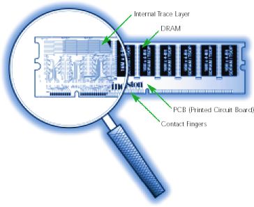
Memory comes in a variety of sizes and shapes. In general, it looks like a flat green stick with little black cubes on it. Obviously, there's a lot more to memory than that. The illustration below shows a typical memory module and points out some of its most important features.
A closer look at a 168-pin SDRAM DIMM.
PCB(PRINTED CIRCUIT BOARD)
The green board that all the memory chips sit on is actually made up of several layers. Each layer contains traces and circuitry, which facilitate the movement of data. In general, higher quality memory modules use PCBs with more layers. The more layers a PCB has, the more space there is between traces. The more space there is between traces, the lesser the chance of noise interference. This makes the module much more reliable.DRAM (DYNAMIC RANDOM ACCESS MEMORY)
DRAM is the most common form of RAM. It's called "dynamic" RAM because it can only hold data for a short period of time and must be refreshed periodically. Most memory chips have black or chrome coating, or packaging, to protect their circuitry. The following section titled "Chip Packaging" shows pictures of chips housed in different types of chip packages.CONTACT FINGERS
The contact fingers, sometimes referred to as "connectors" or "leads," plug into the memory socket on the system board, enabling information to travel from the system board to the memory module and back. On some memory modules, these leads are plated with tin while on others, the leads are made of gold. To learn more about the type of metal on the contacts, refer to the section titled, "Tin versus Gold" on page 67.INTERNAL TRACE LAYER
The magnifying glass shows a layer of the PCB stripped away to reveal the traces etched in the board. Traces are like roads the data travels on. The width and curvature of these traces as well as the distance between them affect both the speed and the reliability of the overall module. Experienced designers arrange, or "lay out," the traces to maximize speed and reliability and minimize interference.CHIP PACKAGING
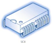
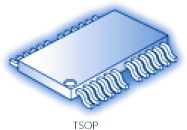
The term "chip packaging" refers to the material coating around the actual silicon. Today's most common packaging is called TSOP (Thin Small Outline Package). Some earlier chip designs used DIP (Dual In-line Package) packaging and SOJ (Small Outline J-lead). Newer chips, such as RDRAM use CSP (Chip Scale Package). Take a look at the different chip packages below, so you can see how they differ.DIP (DUAL IN-LINE PACKAGE)
When it was common for memory to be installed directly on the computer's system board, the DIP-style DRAM package was extremely popular. DIPs are through-hole components, which means they install in holes extending into the surface of the PCB. They can be soldered in place or installed in sockets.
SOJ (SMALL OUTLINE J-LEAD)
SOJ packages got their name because the pins coming out of the chip are shaped like the letter "J". SOJs are surface-mount components - that is, they mount directly onto the surface of the PCB.
TSOP (THIN SMALL OUTLINE PACKAGE)
TSOP packaging, another surface-mount design, got its name because the package was much thinner than the SOJ design. TSOPs were first used to make thin credit card modules for notebook computers.
CSP (CHIP SCALE PACKAGE)
Unlike DIP, SOJ, and TSOP packaging, CSP packaging doesn't use pins to connect the chip to the board. Instead, electrical connections to the board are through a BGA (Ball Grid Array) on the underside of the package. RDRAM (Rambus DRAM) chips utilize this type of packaging.
CHIP STACKING
For some higher capacity modules, it is necessary to stack chips on top of one another to fit them all on the PCB. Chips can be "stacked" either internally or externally. "Externally" stacked chip arrangements are visible, whereas "internally" stacked chip arrangements are not.
Example of externally stacked chips.